Design and Design Automation of Flexible Hybrid Electronics
Wearable Applications are Blossoming
Background
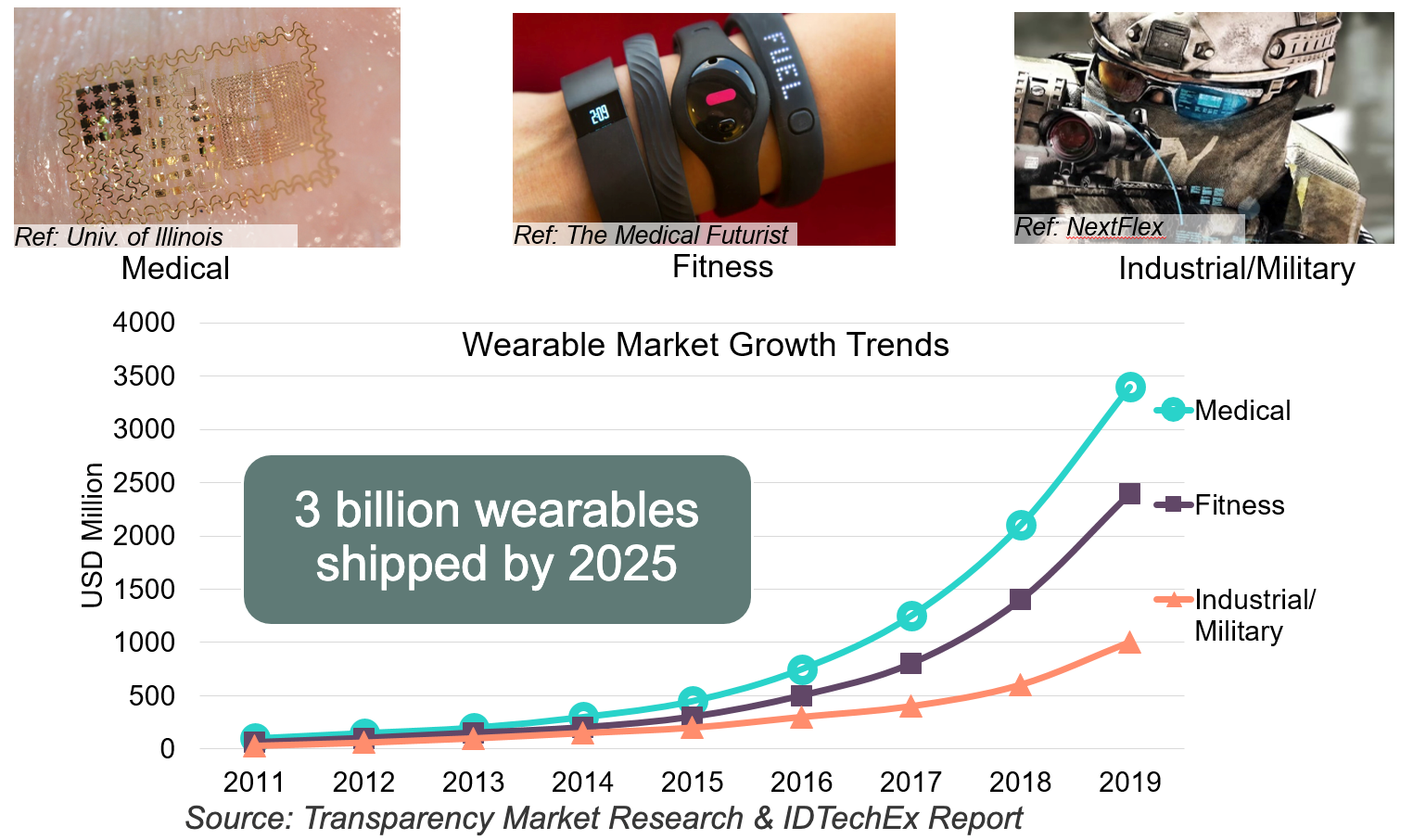
Recent progress of wearable innovations, have attracted more & more attentions, involves
areas from medical, fitness to industries & military. If you look at the bottom chart, it
gives you more precise quantitative analysis. From the chart, you can clearly tell that the
wearable market grows rapidly, especially in recent years, starts from 2015 the annual
growth rate is >50%, and the momentum will keep going, until 2025, IDTechEx estimates that 3
billion wearables will be shipped indicating hundreds of billion $ market. Combining FE with
thinned silicon chips, known as flexible hybrid electronics (FHE), can take advantages of
both low-cost printed electronics and high-performance silicon chips, which brings together
flexible form factors and wearable innovations.
Status
Despite recent advances in the development of flexible materials, devices and integrations
[6, 10], it is still challenging to design a disruptive product using flexible hybrid
electronics (FHE), as illustrated in Figure 1, which involves multiple FHE vendors, silicon
die-thinning and advanced packaging to achieve an ultra-flexible and highly-compact form
factor and the required electrical specifications at the same time. Besides the large
process variations and device defects due to the low cost and low temperature printing
process, FHE applications will also involve bending, stretching and twisting scenarios,
where the electrical characteristics and circuit performance has to been carefully
characterized under different scenarios. To overcome the mentioned design challenges, it
will need advanced design automation techniques to alleviate large process variations [4,
5,7,8], mono-type circuit design challenges [13] and heterogeneous integrations through
accurate electrical models [2,7], robust circuit designs [11,12,13], automatic design rule
checking [8], bending-aware place-and-route and multi-physics analysis [5].

A conceptual diagram of an FHE patch that includes printed sensors, sensor peripheral
circuits, printed super capacitors, printed antennas and thinned silicon chips, which offers
greater comfort (wear-and-forget), enables continuous and non-invasive health monitoring,
and could possibly be disposable once it reaches the economy of scale.
Current and Future Challenges
The complexity of FHE design not only caused by device level variations and limited device
performances (only mono-type of printed transistors are available, either p- or n- type
[13]), but also rises from the requirements of multi-physics considerations, multiple supply
vendors and complicate board-level packaging, as shown in the top of Fig. 2, which
inevitably leads to multiple iterations in order to simultaneously achieve the desired
performance, flex form factors and a high yield. As illustrated in Fig. 2, Process Design
Kit (PDK) [5,7,8], as the enabler and interface between manufactures and designers, serves
as the database including electrical/multi-physics models, design rules and material
information collected from various vendors, thus it can decouple the designers from tedious
back-end processing and reduce the design circles. The PDK for FHE is aimed to facilitate
the entire design flow covering electrical design, multi-physics design rule checking and
the control of manufacturing yield, which differentiates FHE-PDK from the silicon
counterpart facilitating only the electrical design.
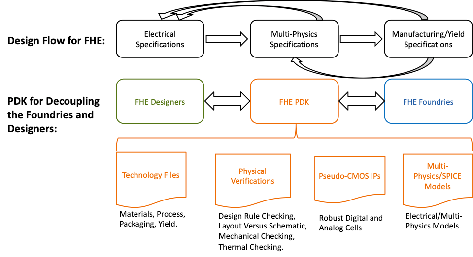
Design Ecosystem of Flexible Printed Electronics: The FHE design flow covers electrical
designs, multi-physics specifications and manufacturing considerations, which will need
multiple iterations to achieve the desired electrical performance, great mechanical
flexibilities and a high yield. Process Design Kit (PDK) severs as the interface between
foundries and designers, which is aimed to decouple the backend process and FHE designs and
reduce the required design iterations and cost.
Several demonstrations have been made to show the potential of FHE for high-fidelity
skin-senor-silicon interfacing and scalable large area sensing system with customized PDK
and design automation flow [1, 3], however, more efforts and innovations are needed in
robust flexible circuit design, bending-aware place and route (P&R) and multi-physics
analysis.
Project Highlights


Nature Communication 2019: With the help of the developed model and Pseudo-CMOS design, we
successfully designed the Pseudo-CMOS cell library: invert NAND XOR gates, ring oscillators;
& Sequential circuit: DFF Shift register. All of them will be open sourced to facilitate the
FHE society. For complexity wise, we achieved 8-stage SR with more than 400 TFTs; For speed
wise, our ring oscillator can run at 3.5 MHz and the stage delay is 28ns. Taking both speed
& complexity into account, we show the best results comparing to the state-of-art CNT
results. It is the joint efforts of high performance CNT devices, PDK development and
Pseudo-CMOS design to make this happen.
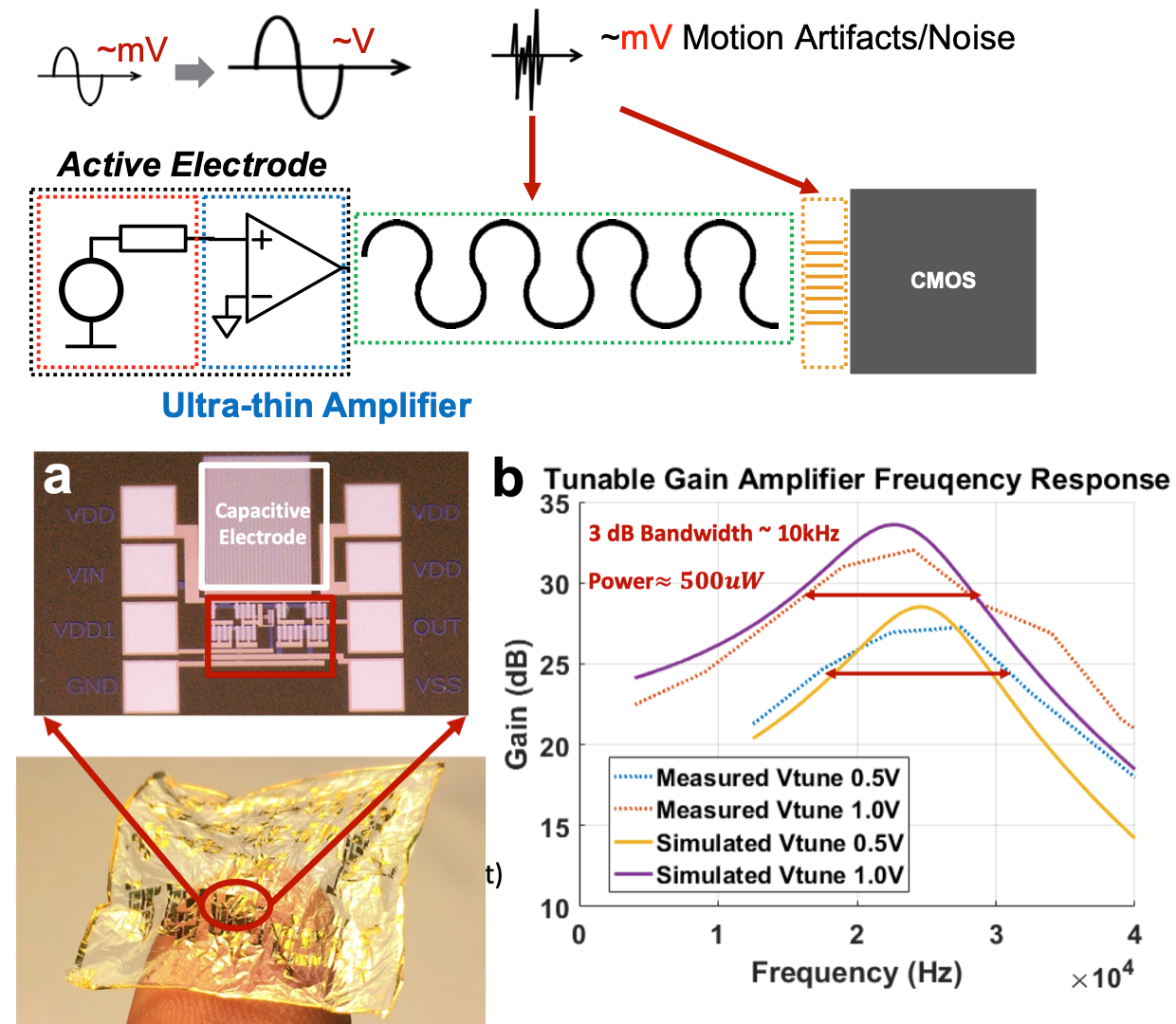
DAC 2019: Skin-inspired electronics emerges as a new paradigm due to the increasing demands
for conformable and high-quality skin-sensor-silicon (SSS) interfacing in wearable,
electronic skin and health monitoring applications. Advances in ultra-thin, flexible,
stretchable and conformable materials have made skin electronics feasible. In this paper, we
prototyped an active electrode (with a thickness≤ 2 um), which integrates the electrode with
a thin-film transistor (TFT) based amplifier, to effectively suppress motion artifacts. The
fabricated ultra-thin amplifier can achieve a gain of 32 dB at 20 kHz, demonstrating the
feasibility of the proposed active electrode. Using atrial fibrillation (AF) detection for
electrocardiogram (ECG) as an application driver, we further develop a simulation framework
taking into account all elements including the skin, the sensor, the amplifier and the
silicon chip. Systematic and quantitative simulation results indicate that the proposed
active electrode can effectively improve the signal quality under motion noises (achieving
≥30 dB improvement in signal-to-noise ratio (SNR)), which boosts classification accuracy by
more than 19% for AF detection.


DAC 2020: Large area flexible electronics (FE) is emerging for low-cost, lightweight
wearable electronics, artificial skins and IoT nodes, benefiting from its low-cost
fabrication and mechanical flexibility. However, the low temperature requirement for
fabrication on a flexible substrate and the large-area nature of flexible sensor arrays
inevitably result in inadequate device yield, reliability and stability.
Therefore, it is essential to develop design methodologies for large area sensing
applications which can ensure system robustness without relying on highly reliable devices.
Based on the observation that most signals sensed by body sensor arrays exhibit sparse
statistical characteristics, we propose a system design method which leverages the sparse
nature via compressed sensing (CS). Specifically, we use flexible circuitry to implement a
CS encoder and decode the compressed signal in the silicon side. As a system demonstration,
we fabricated the temperature sensor array, shift register and amplifier to illustrate the
feasibility of the encoder design using carbon-nanotube-based flexible thin-film
transistors.
Publication:
[1] Shao, L., Lei, T., Huang, T. - C., Bao, Z., and Cheng, K. - T., “Robust Design of Large Area Flexible Electronics via Compressed Sensing”, in 57th Design Automation Conference (DAC), 2020.
[2] Shao, L., Huang, T. - C., Lei, T., Chu, T.-Y., Bao, Z., Beausoleil, R., Wang, M. and Cheng, K. - T., “Compact Modeling of Thin Film Transistors for Flexible Hybrid IoT Design”, in IEEE Transaction of Design & Test, 2019.
[3] Shao, L., Li, S., Lei, T., Huang, T. - C., Beausoleil, R., Bao, Z., and Cheng, K. - T., “Ultra-thin Skin Electronics for High Quality and Continuous Skin-Sensor-Silicon Interfacing”, in 56th Design Automation Conference, 2019.
[4] Y. Wang, Shao, L., Lastras-Montano, M. Angel, and Cheng, K. - T. Tim, “Taming Emerging Devices’ Variation and Reliability Challenges with Architectural and System Solutions”, in 32nd IEEE International Conference on Microelectronic Test Structures (Invited Paper), Kita-Kyushu City, Japan, 2019.
[5] T. - C. Jim Huang, Lei, T., Shao, L., Sivapurapu, S., Swaminathan, M., Li, S., Bao, Z., Cheng, K. - T. Tim, and Beausoleil, R. G., “Process Design Kit and Design Automation for Flexible Hybrid Electronics”, in Design Automation And Test in Europe (Invited Paper), Florence, Italy, 2019.
[6] Lei, T., Shao, L. (Co-first), Zheng, Y., Pitner, G., Fang, G., Zhu, C., Li, S., Huang, Beausoleil, R., Wong, H. - S., Huang, T. - C., Cheng, K. - T., and Bao, Z. “Low-voltage High-performance Flexible Digital and Analog Circuits based on Ultrahigh-purity Semiconducting Carbon Nanotubes”, in Nature Communication, 2019.
[7] Shao, L., Lei, T., Huang, T. - C., Beausoleil, R., Bao, Z., and Cheng, K. - T., “Compact Modeling of Carbon Nanotube Thin Film Transistors for Flexible Circuit Design”, Best Paper Awards Nomination, in Design, Automation and Test in Europe (DATE), Dresden, Germany.
[8] Shao, L., Lei, T., Huang, T. - C., Beausoleil, R., Bao, Z., and Cheng, K. - T., “Process Design Kit for Flexible Hybrid Electronics”, (Invited paper) in 23rd Asia and South Pacific Design Automation Conference (ASP-DAC).
[9] Shao, L., Chu, T. - Y., Tao, Y., and Cheng, K. - T. Tim, “Fully Printed Organic Pseudo-CMOS Circuits for Sensing Applications”, in 1st IEEE International Flexible Electronics Technology Conference (IFETC), Ottawa, Canada.
[10] Lei, Ting, et al. "Biocompatible and totally disintegrable semiconducting polymer for ultrathin and ultralightweight transient electronics." in Proceedings of the National Academy of Sciences 114.20 (2017): 5107-5112.
[11] Huang, T. - C., Shao, L., Lei, T., Beausoleil, R. G., Bao, Z., and Cheng, K. - T. Tim, “Robust Design and Design Automation for Flexible Hybrid Electronics”, in International Symposium on Circuits and Systems (ISCAS), 2017.
[12] T. - C. Huang, J. -L. Huang, and K. -T. Cheng, "Design, Automation, and Test for Low-Power and Reliable Flexible Electronics", Foundations and Trends in Electronic Design Automation, vol. 9, pp. 99-210, 2015.
[13] Huang, Tsung-Ching, et al. "Pseudo-CMOS: A design style for low-cost and robust flexible electronics." in IEEE Transactions on Electron Devices 58.1 (2010): 141-150.